SE98A_4
?NXP B.V. 2009. All rights reserved.
Product data sheet
Rev. 04 25 November 2009
5 of 43
NXP Semiconductors
SE98A
DDR memory module temp sensor, 1.7 V to 3.6 V
7. Functional description
7.1 Serial bus interface
The SE98A uses the 2-wire serial bus (I
2
C-bus/SMBus) to communicate with a host
controller. The serial bus consists of a clock (SCL) and data (SDA) signals. The device
can operate on either the I
2
C-bus Standard/Fast mode or SMBus. The I
2
C-bus
Standard-mode is defined to have bus speeds from 0 Hz to 100 kHz, I
2
C-bus Fast-mode
from 0 Hz to 400 kHz, and the SMBus is from 10 kHz to 100 kHz. The host or bus master
generates the SCL signal, and the SE98A uses the SCL signal to receive or send data on
the SDA line. Data transfer is serial, bidirectional, and is one bit at a time with the Most
Significant Bit (MSB) transferred first, and a complete I
2
C-bus data is 1 byte. Since SCL
and SDA are open-drain, pull-up resistors must be installed on these pins.
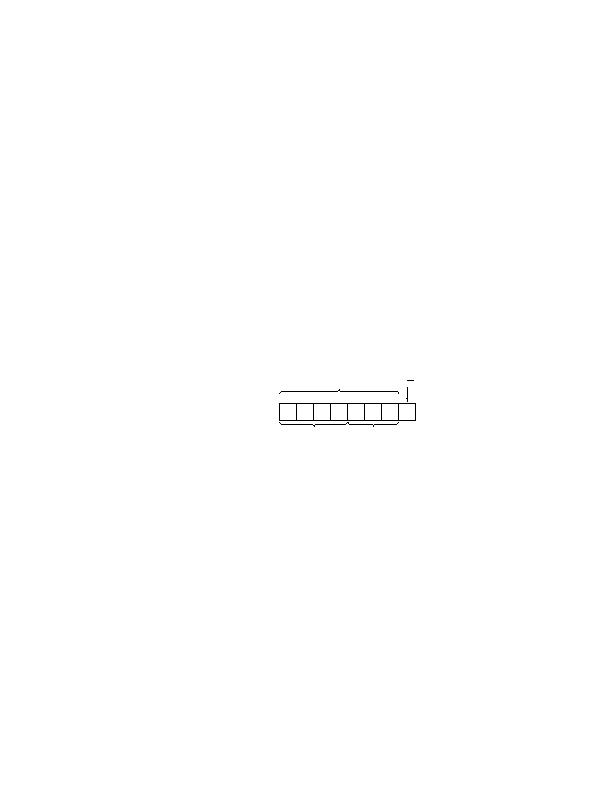
7.2 Slave address
The SE98A uses a 4-bit fixed and 3-bit programmable (A0, A1 and A2) 7-bit slave address
that allows a total of eight devices to coexist on the same bus. The input of each pin is
sampled at the start of each I
2
C-bus/SMBus access. The A0, A1 and A2 pins are pulled
LOW internally. The A0 pin is also overvoltage tolerant, supporting 10 V software write
protection when applied to the SPD that shares common address lines.
Fig 5. Slave address
R/W
002aab304
0
0
1
1
A2
A1
A0
fixed
hardware
selectable
slave address
MSB
LSB
X
发布紧急采购,3分钟左右您将得到回复。
相关PDF资料
SG6901ASZ
IC PFC CTLR AVERAGE CURR 20SOIC
SG6932SZ
IC PFC CONTROLLER CCM 16SOP
SG6961SY
IC PFC CTRLR AVERAGE CURR 8SOIC
SI3500-A-GM
IC POE SWITCH PWR OVER LAN 20QFN
SI786LSG-E3
IC REG QD BUCK/LINEAR 28SSOP
SIC417CD-T1-E3
IC REG DL BCK/LINEAR SYNC 32MLPQ
SP619EK-L/TR
IC HIGH CURRENT SW SOT23-6
TC573302ECTTR
IC REG CTRLR SGL 3.3V SOT23A-5
相关代理商/技术参数
SE98PW
制造商:PHILIPS 制造商全称:NXP Semiconductors 功能描述:SO-DIMM SMBus/I2C-bus temperature sensor
SE98PW,118
功能描述:板上安装温度传感器 I2C LOCAL +/- 2OC RoHS:否 制造商:Omron Electronics 输出类型:Digital 配置: 准确性:+/- 1.5 C, +/- 3 C 温度阈值: 数字输出 - 总线接口:2-Wire, I2C, SMBus 电源电压-最大:5.5 V 电源电压-最小:4.5 V 最大工作温度:+ 50 C 最小工作温度:0 C 关闭: 安装风格: 封装 / 箱体: 设备功能:Temperature and Humidity Sensor
SE98PW-T
功能描述:板上安装温度传感器 I2C LOCAL +/- 2OC TS DIMM RoHS:否 制造商:Omron Electronics 输出类型:Digital 配置: 准确性:+/- 1.5 C, +/- 3 C 温度阈值: 数字输出 - 总线接口:2-Wire, I2C, SMBus 电源电压-最大:5.5 V 电源电压-最小:4.5 V 最大工作温度:+ 50 C 最小工作温度:0 C 关闭: 安装风格: 封装 / 箱体: 设备功能:Temperature and Humidity Sensor
SE98TK
制造商:PHILIPS 制造商全称:NXP Semiconductors 功能描述:DDR memory module temp sensor, 3.3 V
SE98TK,118
功能描述:板上安装温度传感器 I2C LOCAL +/- 2OC RoHS:否 制造商:Omron Electronics 输出类型:Digital 配置: 准确性:+/- 1.5 C, +/- 3 C 温度阈值: 数字输出 - 总线接口:2-Wire, I2C, SMBus 电源电压-最大:5.5 V 电源电压-最小:4.5 V 最大工作温度:+ 50 C 最小工作温度:0 C 关闭: 安装风格: 封装 / 箱体: 设备功能:Temperature and Humidity Sensor
SE98TK-T
功能描述:板上安装温度传感器 I2C LOCAL +/- 2OC TS DIMM RoHS:否 制造商:Omron Electronics 输出类型:Digital 配置: 准确性:+/- 1.5 C, +/- 3 C 温度阈值: 数字输出 - 总线接口:2-Wire, I2C, SMBus 电源电压-最大:5.5 V 电源电压-最小:4.5 V 最大工作温度:+ 50 C 最小工作温度:0 C 关闭: 安装风格: 封装 / 箱体: 设备功能:Temperature and Humidity Sensor
SE9E1210A1.5-4R
制造商:JOSLYN 功能描述: 制造商:JOSLYN SUNBANK COMPANY LL 功能描述:
SE9ESA847R100
制造商:Lanner Electronics Inc 功能描述:WALL MOUNT-2 V1.0
